I’ve finished laying out the base station PCB, hurrah!
As ever I’ve laid it out using Eagle – this time I’ve managed to keep it to two layers so that’ll save me some money in PCB manufacture costs. Click it to enlarge.
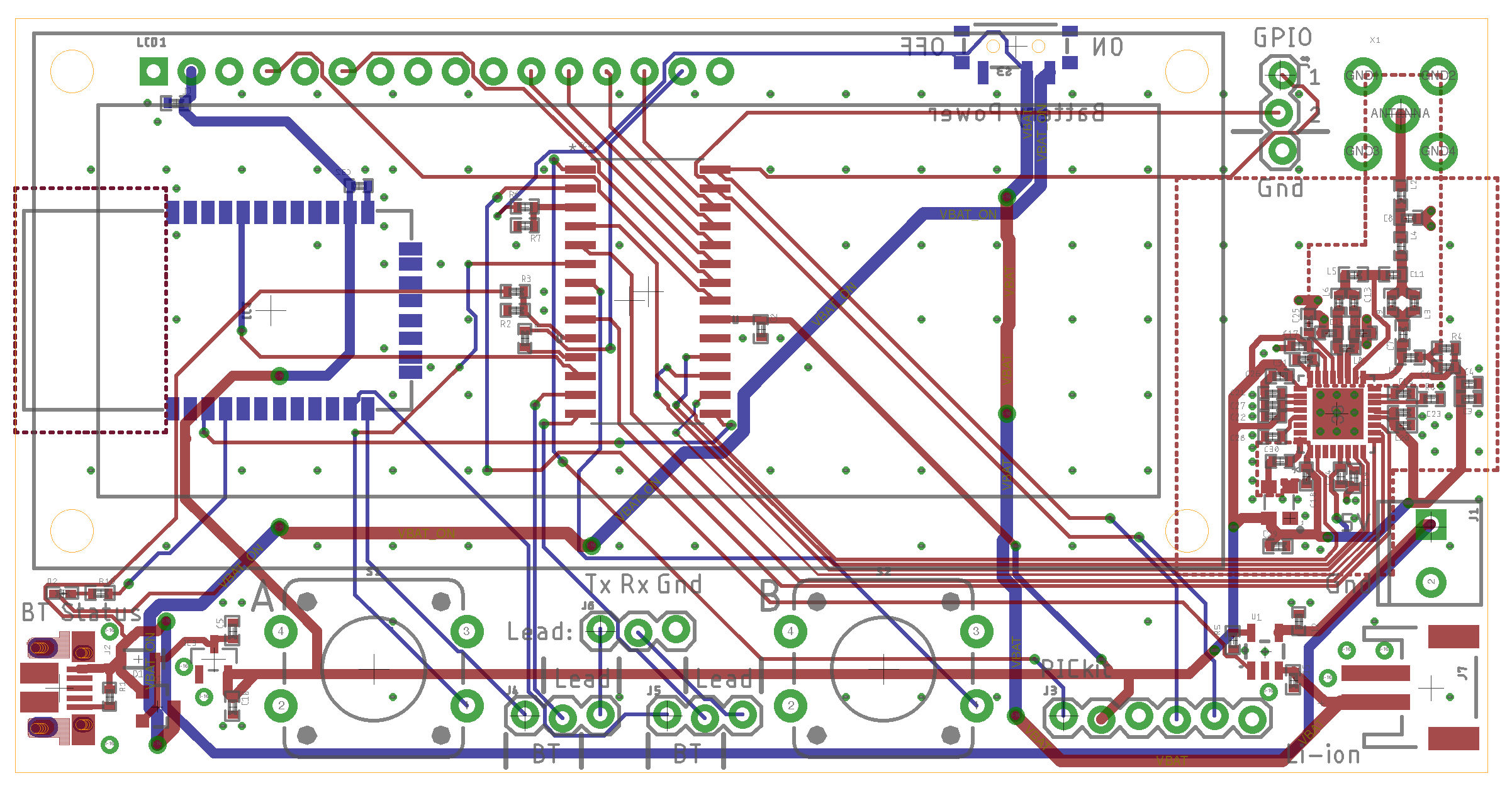
The CC1125 transceiver IC is on the right hand side of the PCB – I’ve made sure to keep the ground plane underneath the CC1125 free from other tracks such that the IC has an unbroken ground reference. This is good (essential!) RF practice.
There is however some good (essential?!) RF practice that I’ve not followed. oshpark.com (my favourite fab) have two options for 2-layer PCB heights, 0.8mm or 1.6mm. In an ideal world, calculations show that for a 0.8mm height FR4 (er = 4.5) substrate, the 50 ohm PCB trace width needs to be 1.5mm. This is completely unworkable for my design as I’d end up with really wide traces constantly getting necked down into tiny 0402 components. It’d take up a great deal of space and look ridiculous! So instead what I’ve done is arbitrarily set the trace width to the width of the 0402 pads. This means that the trace is one constant width all the way from the CC1125 to the antenna. Simulations I’ve carried out in Microwave Office show that in most cases the insertion loss and return loss (S21 and S11) of the trace are actually better if you set your trace width to a constant, “incorrect” value rather than setting the width to the correct 50 ohm value (1.5mm in my case) and every few mm having it neck down into 0402 components. The discontinuities this causes outweighs the fact that the trace width is the “correct” value.
Usually you’d ensure that you choose your substrate height such that the 50 ohm trace width is around the same as the width of the component pads you are using. Unfortunately I don’t have that luxury with oshpark given than 0.8 mm is the smallest height they do for 2-layer PCBs. This wasn’t an issue for the main CatTrack board because it was a 4-layer PCB and the height between layers 1 and 2 (used as the ground reference) was only 0.17 mm. This results in much more convenient values on layer 1 for 50 ohm trace widths.
I’ve tried to stick to using components from the SparkFun PCB libraries, just because I can be reasonably sure that the footprints will be accurate. They even come built-in to the latest versions of Eagle, so that’s handy.
The switches I’m using to control the base station can be seen in the bottom middle of the PCB – I’ve marked them A and B in the silkscreen.
The RN41 Bluetooth module is on the back of the PCB and I’ve cleared both grounds around the antenna on the RN41 board in order that the antenna can radiate properly.
I’m using a 16×2 LCD screen as a user interface – you should be able to see the 16 pin connector for it in the top left of the PCB. The LCD will sit on pillars on top of the PCB, covering up most of the board, with the two switches underneath it.
I think that’s about it – time to order the PCBs and then get soldering!
One comment