The PCBs have arrived from OSH Park! As expected, they look good and the quality is excellent. As an added bonus, they even fit in the case I designed them for. Result!
Over the last couple of weeks I have also been ordering all the components from a combination of Farnell and tme. Everything’s arrived and it’s all ready to solder into place. I’ve also got the firmware into a state such that something should work too.
Now it’s time to get soldering!
Soldering
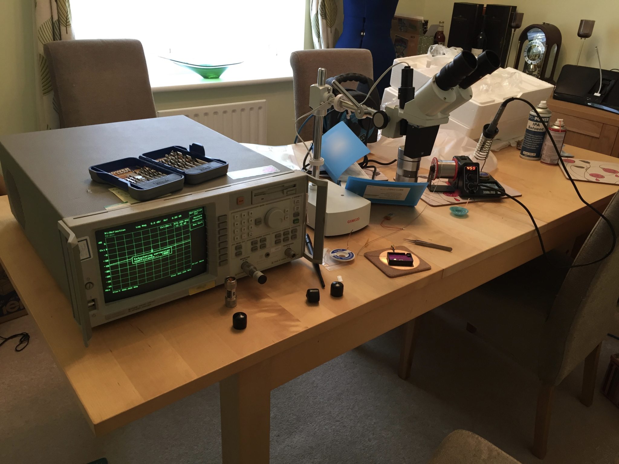 This is my soldering station (my wife calls it the Dining Room). On the left is my Vector Network Analyser (VNA) – this is what is used to get the antenna match right. We want to ensure we transfer the maximum possible amount of power from the output stage of the CC1125 into the antenna. I’ve also got a microscope – it cost me around £200, so it’s not the world’s best microscope, but it makes soldering a large collection of 0402 components a lot easier. My soldering iron is pretty poor – it is a thermostatic one, but even the smallest ground plan can pull the heat out of the iron quicker than it can pump the heat back in. I’ll get myself a better one one day! I used to solder 0402 with a huge iron from Maplin, so although my current one is a bit rubbish, it’s a huge step up.
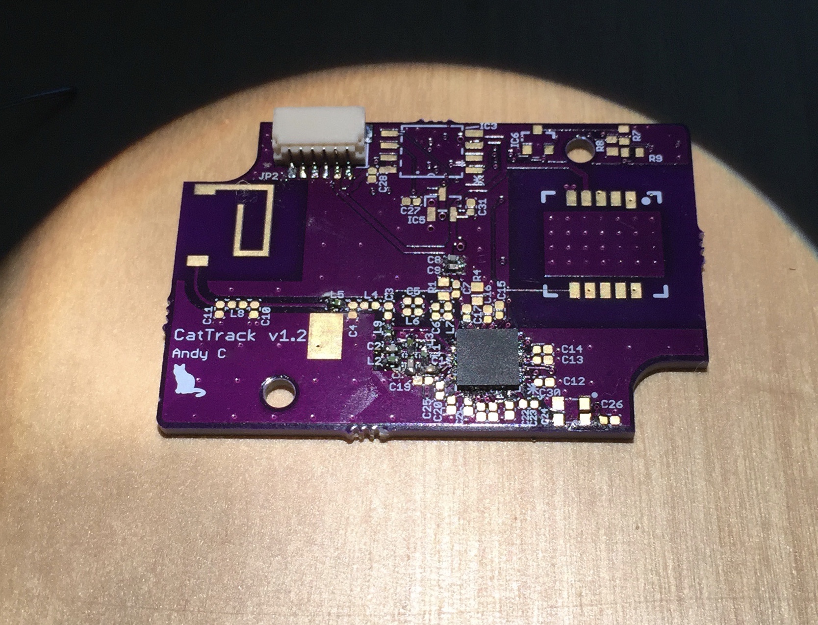
The most difficult component to solder is the CC1125. This is because it’s a QFN device with a ground paddle. There are plenty of youtube videos on how to solder these devices. I put a small amount of solder on each of the pads, then used a hot air gun to pre-heat the board. Once heated I placed the device down and continued to heat from above. This causes the solder to melt and create a good contact with the ground paddle and pads.
The first thing I want to do once it’s all soldered is to measure the output power of the CC1125. In order to do this I’ve connected a small SMA RF lead to the CC1125 output, using the area of copper next to ‘v1.2’ that I’ve purposely not covered in solder resist as a ground plan. I’ve written some basic code in the PIC that tells the CC1125 to output a Continous Wave (CW) at 868 MHz, to allow me to take my measurement. The value we are looking for is 15.0 dBm – the advertised power from the CC1125.
Let’s see how we get on…
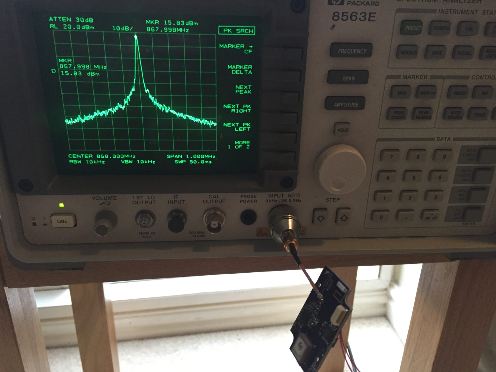
Hurrah! 15.83 dBm! A great relief… it means that I’ve probably soldered everything correctly and got all the right inductor/capacitor values on the CC1125 output.
Antenna Match
The last and often most time-consuming job. I’ve left it to last because it can be affected by pretty much everything else. We need to make sure we adjust the match with all of the components soldered in place, in the final enclosure.
As I’ve said previously, we need to ensure that we get the maximum power transfer from the CC1125 into the antenna. If you just whack the chip antenna on the board and connect it directly to the CC1125 output then nothing will happen – you won’t be transmitting any power at all. Most of the power will end up reflected back into the CC1125. By implementing a correct antenna match we can ensure that there is very little power reflected back into the CC1125, and the maximum amount of power makes it into the antenna.
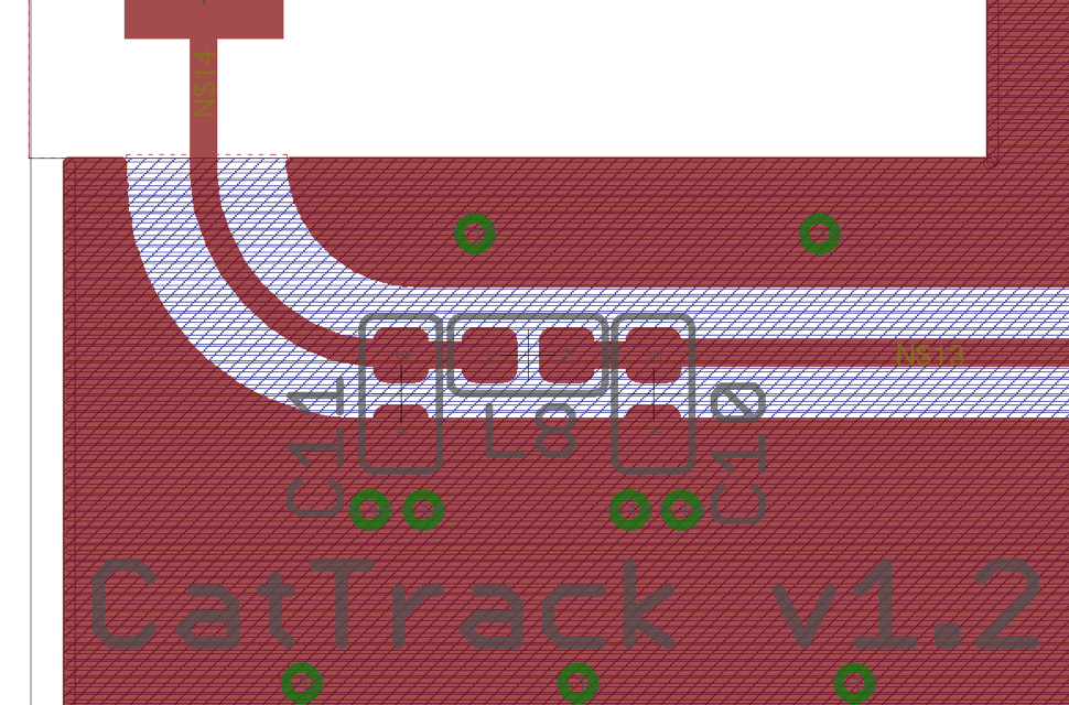
I’ve left this ‘pi’ configuration on the PCB: C11, L8 and C10. A combination of capacitors and inductors will form the matching circuit. The best place to start is the example values given on the datasheet.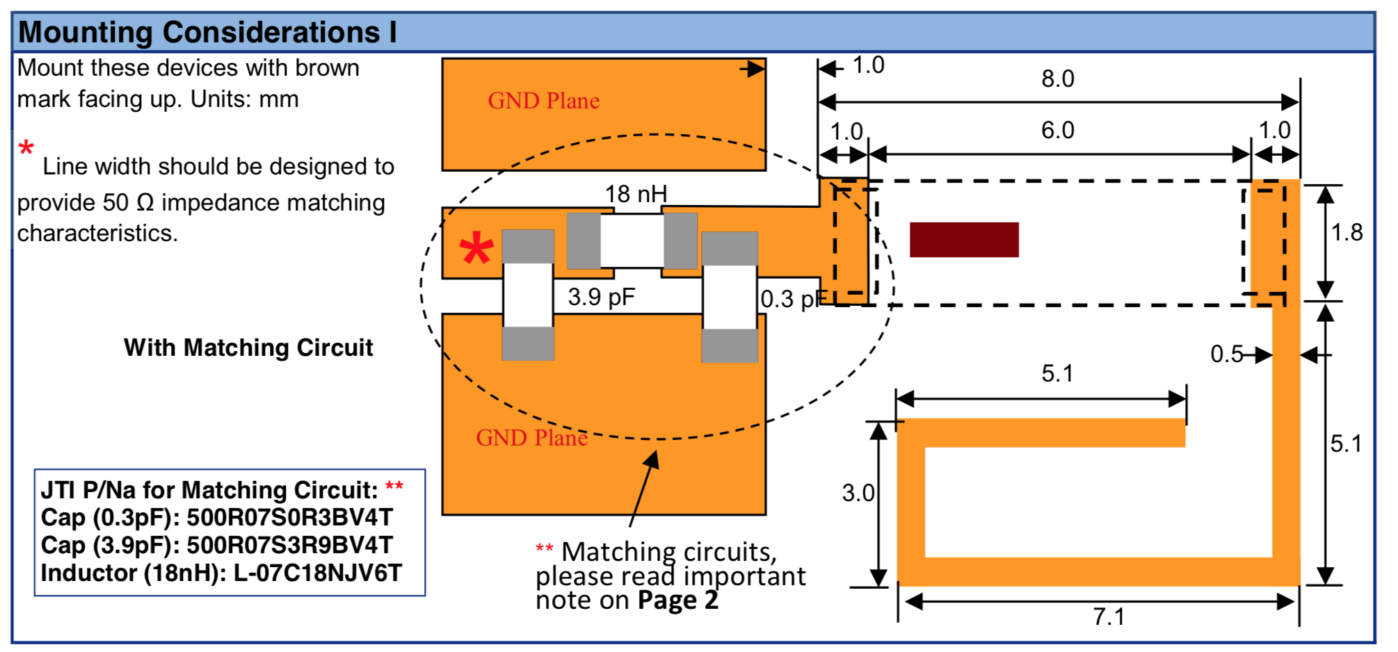
As we can see, a series inductor of 18 nH and a shunt capacitor of 3.9 pF is Johanson’s recommendation. We’ll ignore the 0.3 pF capacitor for now – that will only bring the frequency in ever so slightly, so we can see where we get to just using the two elements then see if it needs a final tweak.
In order to measure the match, I have connected the VNA to the ‘input’ port of the antenna, with the CC1125 output disconnected from it. We know that the CC1125 is matched to 50 ohms, so we will now match the antenna to 50 ohms at our design frequency of 868 MHz. That way when we connected them both back together, there will be maximum power transfer between them.
The VNA tells us how much power is being reflected back from the antenna at each frequency. Simplistically speaking, we are looking for a deep notch on the VNA display at 868 MHz. This tells us that at this frequency all of the power is going into the antenna and very little is being reflected back. We could also use a Smith chart to get a more accurate view of what’s happening, but that’s probably a little complex to explain here!
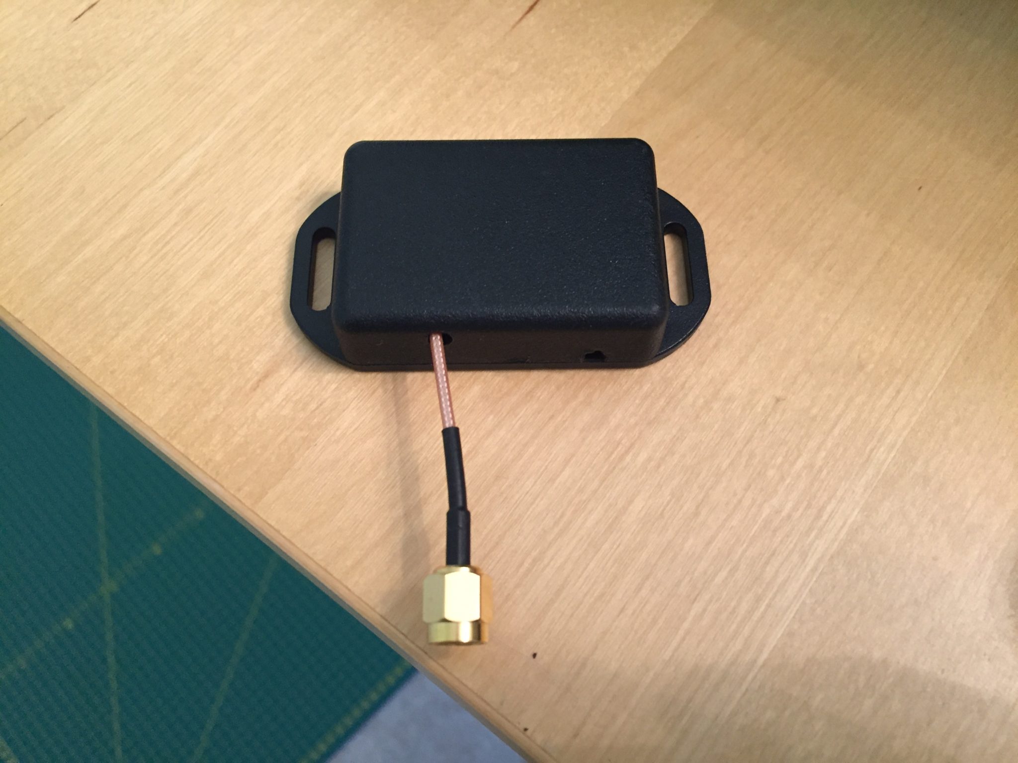
We also want to ensure that the conditions are as realistic as possible, so we want to measure the match with the PCB inside its case. To that end, I’ve had to make some modifications to one of the cases…!
At first, with the 18 nH series inductor and 3.9 pF shunt capacitor, the match was well off – it was resonating around 950 MHz – nowhere near the 868 MHz we’re after. At this point, with a fairly simple design like this, I tend to just start adjusting the values whilst watching what happens on the VNA. You can soon get a feel for how much each component variation alters the match. Broadly speaking, adjusting the capacitor will alter the match at a specific frequency (the notch will get shallower or deeper), and the inductor will adjust the frequency.
After 15 minutes or so of fiddling, I found that I had to switch to a series capacitor and a shunt inductor. This becomes obvious as you continue to reduce the inductor value, but you can’t bring the frequency down far enough.
I eventually settled on a series capacitor of 1.2 pF and a shunt inductor of 6.8 nH.
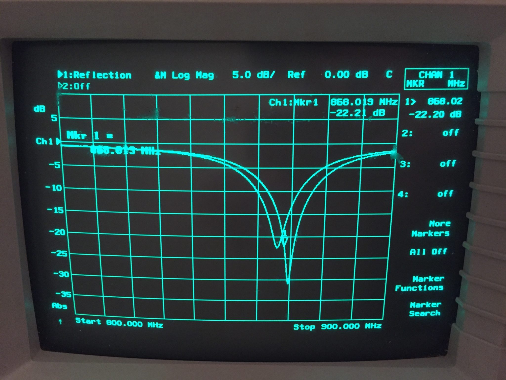
As you can see I’ve got two traces on the display. One is a saved trace and the other is a live trace. I like to save a trace of the match once it’s complete, then wiggle the board around and hold it up to my skin (or a cat!) and check that the notch frequency of the live trace doesn’t deviate too much from the design frequency. A bit of ‘liveliness’ in the notch as you bring your hand in its vicinity is a really good sign that the antenna is radiating well.
Our marker at 868 MHz on the display shows that we are getting a match of 22.21 dB into the antenna. This means that the power reflected back from the antenna is 22.21 dB lower than the power going in. This is very good indeed! Usually you’d consider an antenna ‘good’ if you had a match of 10 dB or better. We do need to just bear in mind that this is a very narrow-band match, so it’s much easier to get a nice deep notch than it is with a wider-band match.
There are all sorts of fancy pieces of software to help with this process – AnTune is a good example.
Phew! Time now to finish the firmware and then get it tested it out on Buttons for real!!
I enjoyed reading this post, thank you for explaning and sharing everything in detail . I hope to see the complete device and in action. How far will you be able to track him?
Hi Eric! The distance I’ll be able to track him from will ultimately end up depending on the antenna position both on him and on the base unit. I would think that if I can get the base unit antenna up nice and high and he is in a favourable position, then I could get around a mile. In practice I think it’ll be around 200-300 metres, assuming he’s in a bush with his head down covering the antenna. More than enough to be able to find him!