Before designing the PCB I need to decide on an enclosure to use. Ideally I need something plastic, with flanges such that it can be attached easily to a cat’s collar. Clearly size will be a big factor – I want something small, but not so small that the chip antenna is ineffective, or that it’s a nightmare to lay out and fit everything in.
After a bit of searching on Farnell, I found this box from Hammond – a big name in the enclosures business! It’s 50mm x 35mm x 15mm and has a plastic flange – perfect for attaching to Buttons’ collar.
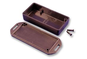
There’s enough space for a small PCB alongside a lithium-ion battery. The dimensions of the box closely match the size of the PCB used by Johanson on their chip antenna development board, so hopefully I’ll be able to get the full performance from the chip antenna.
Very helpfully, Hammond specify the maximum PCB size in their datasheet: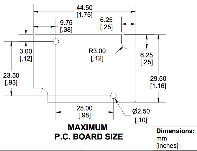
Now I can load this PCB outline directly from the dxf file provided by Hammond into the dimensions layer in my favourite PCB design tool, Eagle.
And then… after a lot of head-scratching later, the PCB is complete!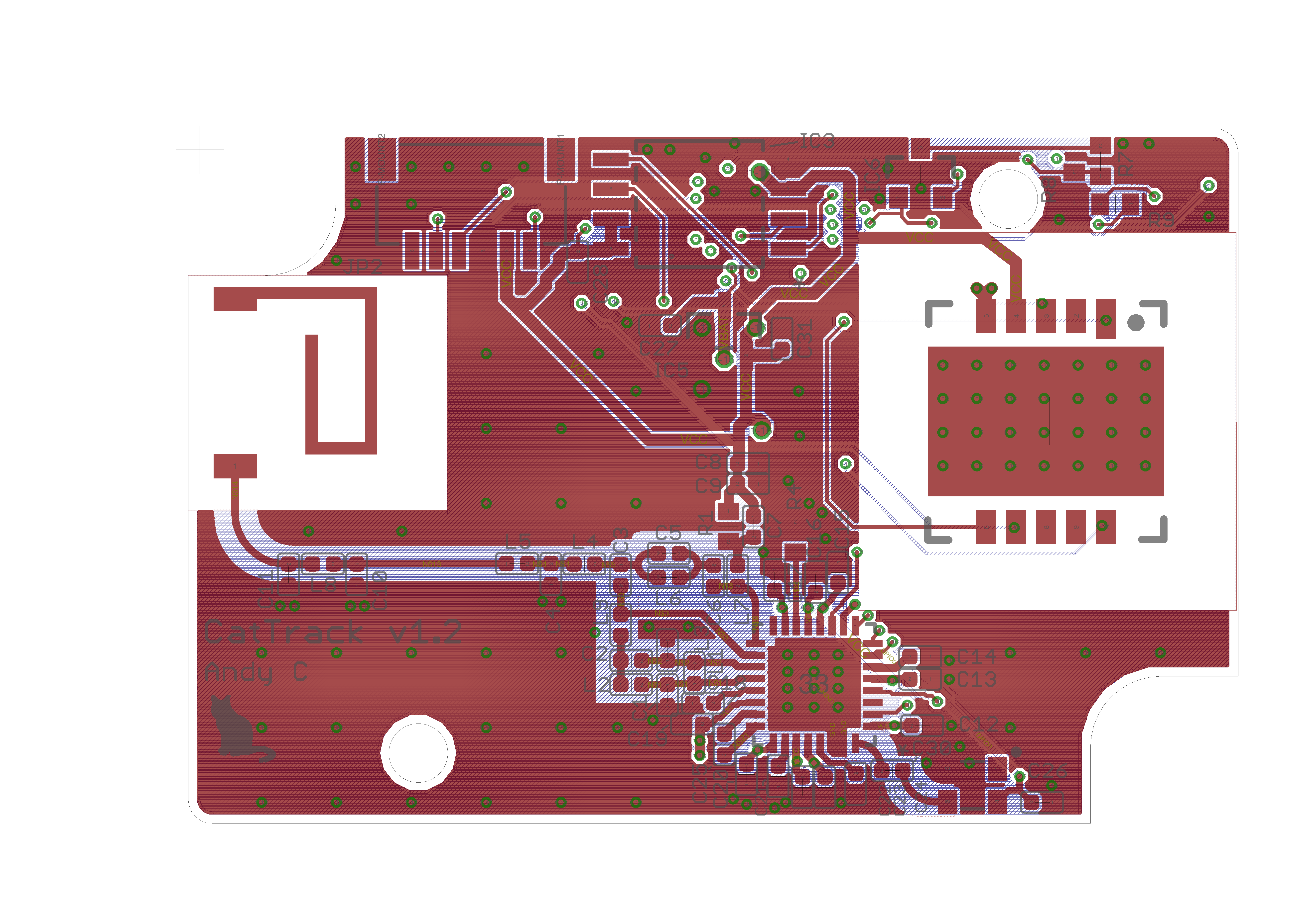
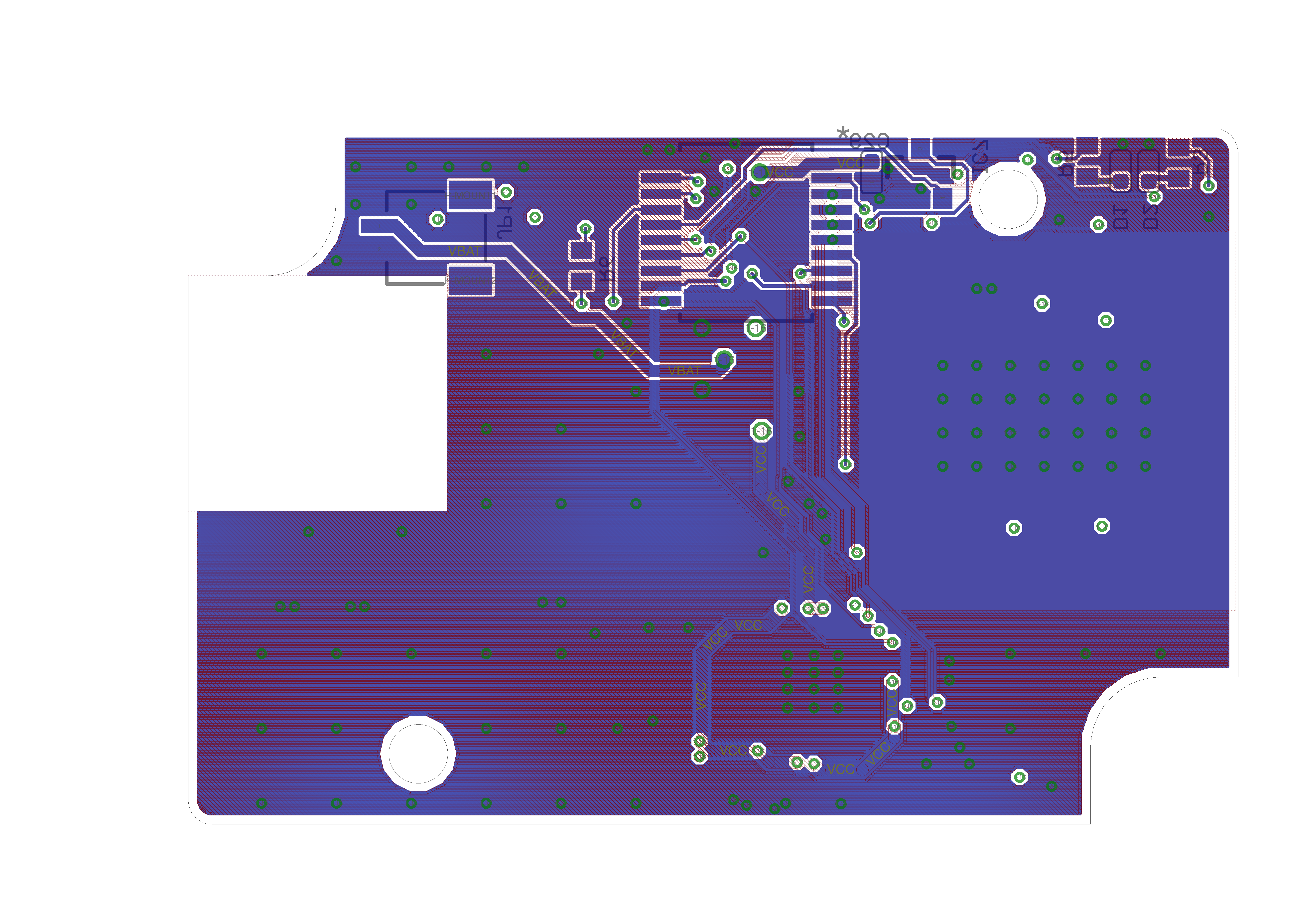 The first image above shows PCB layers 1 and 2, and the image below it shows layers 3 and 4. Click them to enlarge. There was no way that I could have got the design onto a 2 layer PCB, given all the RF circuitry required.
I’ve had numerous PCBs made by OSH Park in the past. They are incredibly inexpensive and very high quality, so I’ll definitely be using them for my CatTrack design.
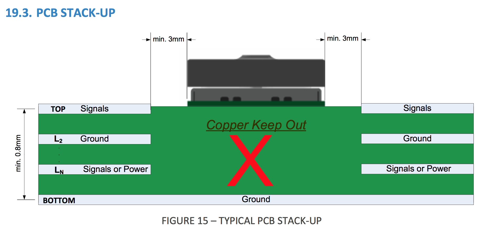
I’ve used layer 2 as a ground reference for all of the RF circuitry around the CC1125 on layer 1, so there is no routing in layer 2 in this area. Additionally I’ve made sure that the RF traces are the correct width for 50 ohm microstrip, using the 4-layer OSH Park stackup, here.
The copper is cleared on all four layers around the antenna, allowing it to radiate effectively. I’ve also cleared the copper from layers 1-3 underneath the GPS module and avoided routing in this area. The GPS module will be using layer 4 as a ground reference. I’ve made sure that I’ve followed the 3mm keep-out area around the GPS module from the datasheet, so hopefully I’ll get some decent performance from the module.
I spent quite a lot of time refining the silkscreen on the PCB (the silkscreen is the white writing that appears on PCBs). It makes life so much easier during soldering and debug if the silkscreen is neat and accurate. Plus it makes the PCB look much better!
Now to send the design files off to OSH Park and wait excitedly by the postbox for the boards to arrive!
One comment